Buck
Buck converter — CCM
A simple step-down converter with continuous inductor current.
1Overview
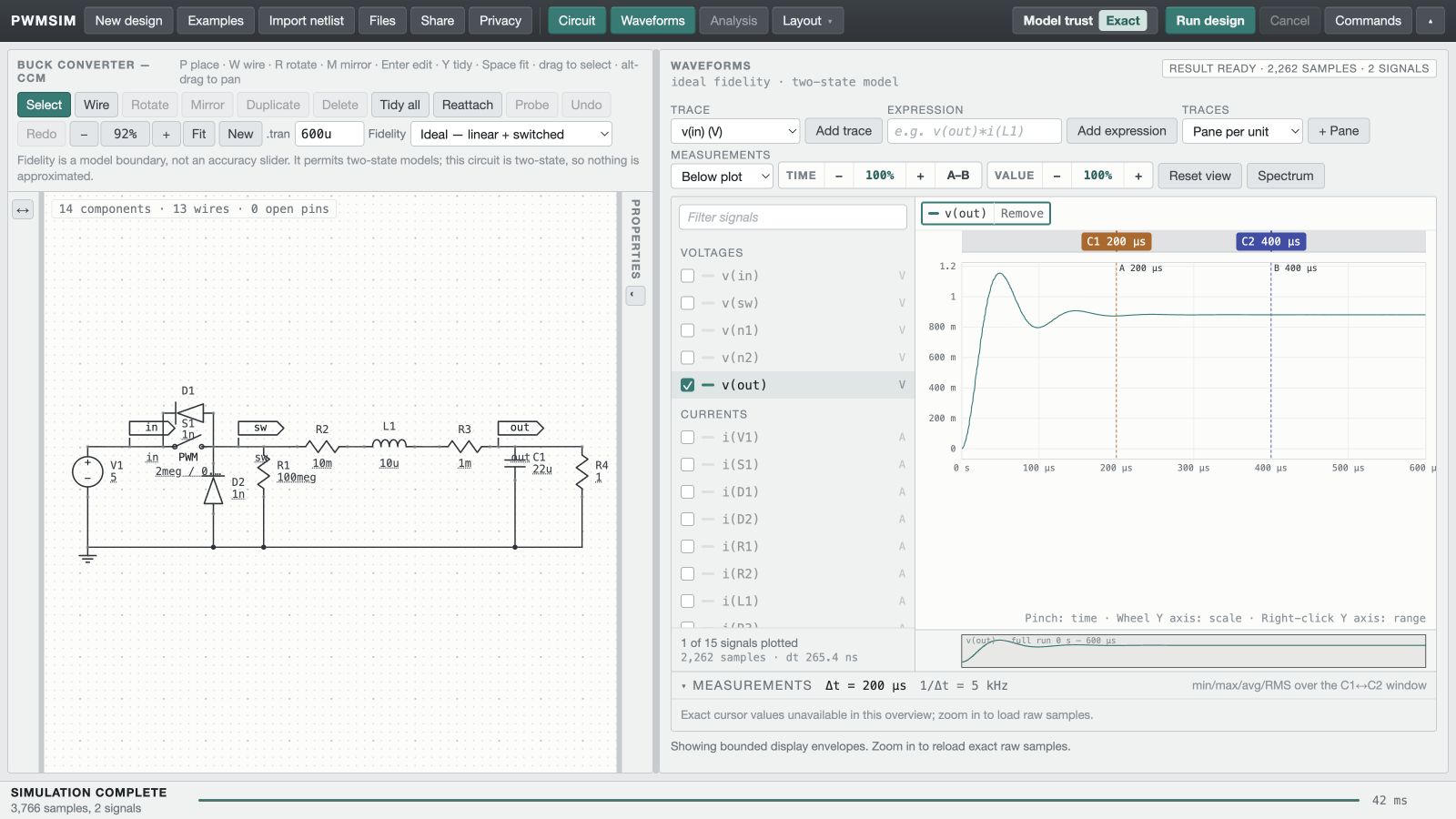
The simplest switching converter in the gallery: a buck (step-down) converter running open loop at a fixed duty cycle. It turns 5 V into about 0.88 V at 2 MHz, and its inductor current never reaches zero, which is continuous conduction mode (CCM).
Use it to learn the app, and to check the textbook buck equations against a simulation: every result below is worked out by hand first.
2Model

S1 connects the input to the switch node sw for a fraction D = 0.18 of each 500 ns period, as PWM1 commands. When S1 opens, D2 carries the inductor current. L1 and C1 filter the switch node into a nearly constant output across the load R4.
The switches and diodes are two-state models (Ideal switched in the app): on, they are a 10 mΩ resistance; off, an open circuit (100 MΩ to 1 GΩ). The diode's forward drop is 1 nV, so it is ideal in practice. R2 and R3 add the inductor's and the trace's resistance.
| Part | Kind | Value | Role |
|---|---|---|---|
| V1 | DC voltage | 5 | Input source |
| S1 | Switch | — | Main switch |
| PWM1 | PWM | 2 MHz · 18% | Gate signal for S1 |
| D1 | Diode | 1n | Body diode of S1 |
| D2 | Diode | 1n | Freewheeling diode |
| R1 | Resistor | 100meg | Keeps the switch node defined |
| R2 | Resistor | 10m | Inductor resistance |
| L1 | Inductor | 10u | Output inductor |
| R3 | Resistor | 1m | Trace resistance |
| C1 | Capacitor | 22u | Output capacitor |
| R4 | Resistor | 1 | Load |
3How it works
Output voltage
In steady state the inductor's average voltage is zero (volt-second balance). During the on-time it sees Vin − Vout, during the off-time −Vout, so
That gives 0.18 × 5 V = 0.90 V. The load current also flows through 21 mΩ of series resistance (the switch or the diode, 10 mΩ, plus R2 and R3), which takes a little off:
Inductor ripple
During the on-time the inductor current rises with slope (Vin − Vout)/L for D·T:
Staying in CCM
The current's valley is Iout − ΔIL/2. It reaches zero, and the converter leaves CCM, when the load resistance rises to
Here Rcrit = 48.8 Ω, far above the 1 Ω load.
Start-up
Switched on from zero, L1 and C1 ring at f0 = 1/(2π√(LC)) = 10.7 kHz, damped by the load with Q = R√(C/L) = 1.48. A second-order step response overshoots by exp(−πζ/√(1−ζ²)) = 32% (ζ = 1/2Q), peaking at tp = 1/(2f0√(1−ζ²)) = 49.5 µs.
4Simulation
Open the example and it runs once, for 600 µs (1,200 switching periods). Fig. 2 shows the start-up; Fig. 3 the last four periods, where the inductor current is the triangle the ripple equation describes.
Measured over the last ten periods, against the hand calculations of section 3:
| Quantity | By hand | PWMSim |
|---|---|---|
| Output voltage, mean | 0.881 V | 0.881 V |
| Load current, mean of i(L1) | 0.881 A | 0.881 A |
| Inductor ripple, peak to peak | 37.1 mA | 36.9 mA |
| Inductor current, minimum | 0.863 A | 0.863 A |
| Start-up peak of v(out) | 1.17 V | 1.16 V |
| Time of that peak | 49.5 µs | 49.2 µs |
The steady-state values agree within 0.4%. The start-up estimate is looser: it treats the converter as an LC filter switched onto a step of D·Vin, which ignores the switching itself.
5Try this
Raise the duty cycle
Select PWM1 and change its duty from 0.18 to 0.22, then press Run transient. The output and the ripple both follow the equations of section 3:
| Duty 0.22 | By hand | PWMSim |
|---|---|---|
| Output voltage, mean | 1.077 V | 1.077 V |
| Inductor ripple, peak to peak | 43.1 mA | 42.9 mA |
Lighten the load into DCM
Set R4 to 100 Ω, above Rcrit = 48.8 Ω, and the inductor current now reaches zero every period: discontinuous conduction (DCM). The output is no longer D·Vin; with K = 2L/(R·T) = 0.40 it is
The output time constant grows to RC = 2.2 ms, so open
Settings and set the stop time to 10 ms (type 10m) before you run it.
| R4 = 100 Ω | By hand | PWMSim |
|---|---|---|
| Output voltage, mean | 1.235 V | 1.235 V |
| Inductor current, minimum | 0 A | 28 nA |
6What the model leaves out
- Switches and diodes change state instantly. There are no switching transitions, no reverse recovery, no gate drive and no parasitic capacitance, so the only losses are the on-resistances.
- The open-loop output follows the input and the load: there is no controller. The PI and peak-current examples close the loop.
- A simulation is not a hardware test.
7References
- R. W. Erickson and D. Maksimović, Fundamentals of Power Electronics, 3rd ed., Springer, 2020. Chapter 2 (volt-second balance, ripple) and chapter 5 (discontinuous conduction mode).
- N. Mohan, T. M. Undeland and W. P. Robbins, Power Electronics: Converters, Applications, and Design, 3rd ed., Wiley, 2003. Chapter 7.
Every waveform and simulated number above comes from this example as the app opens it, run by PWMSim.